Tin Diselenide
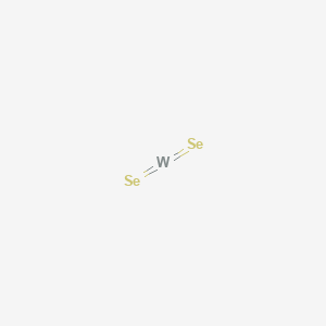
Tin Diselenide is a premium-grade, chemically stable dark gray or black crystalline chalcogenide powder carrying CAS number 1312-11-4. Processed under strict vacuum deposition parameters, this high-purity layered two-dimensional semiconductor exhibits exceptional electron mobility and highly predictable bandgap characteristics, making it an ideal core choice for manufacturing field-effect transistors, advanced photodetectors, and thermoelectric devices globally.
Description
Layered Quantum Mechanics and Optoelectronic Engineering
The immense crystal layer persistence and broad indirect bandgap profiles of Tin Diselenide offer a distinct operational edge in demanding cleanroom lithography and photovoltaic component processing facilities. This crystalline inorganic solid operates by facilitating fast carrier transport kinetics across atomic sub-layers, supplying the exact quantum mechanics required to modulate infrared light reception without altering substrate structural uniformity. It assists processing engineers in maintaining strict thickness profiles across mechanical or liquid exfoliation runs, effectively extending material device stability and preventing premature structural degradation under high electronic current loads. For instance, specialized thin-film factories integrate this selenium compound as a core component to fabricate next-generation photodetector arrays. As a consequence, it maximizes the light conversion sensitivity of automated device networks and satisfies strict nanometer structural tolerances. Consequently, Zyntex coordinates oxygen-free packaging channels to eliminate raw lot degradation variables from your cleanroom storage cabinets.
In addition to this, Zyntex manages tightly regulated climate logistics for high-vacuum equipment brands and specialized energy conversion research laboratories. The substance operates as an active structural block, reacting predictably under laser deposition phases to secure clean crystalline orientations and zero volatile pinhole defects during device layering cycles. It advances modern device engineering by providing a thoroughly verified, highly dependable inorganic chalcogenide that resists ambient atmosphere oxidation when properly enclosed in protective matrices. Simultaneously, it remains a critical chemical standard for routine Raman spectroscopy calibrations and academic crystal lattice validation assays. In brief, our product functions as an indispensable mineral platform, supporting both the commercial performance of solid-state sensors and the analytical accuracy of modern nanotechnology research programs.
Primary Commercial Sectors for Tin Diselenide
This ultra-pure solid crystalline semiconductor delivers crucial technical value within these four critical sectors:
⚡ Optoelectronics
Core base component used to manufacture ultra-sensitive near-infrared photodetectors, optical switch gears, and modern laser sensors. Hence, it directly supports high-efficiency device tracking loops.
🔋 Thermoelectrics
Utilized as a high-performance raw material block to process solid-state waste heat recovery engines and targeted thermal generator lines. Clearly, it is key for uniform lattice energy scores.
🧬 2D Nano-Materials
Functions as an essential crystal matrix source for liquid exfoliation, producing single-layer atomic flakes for quantum research trials. Resultantly, it balances long-term structural phase integrity.
🔬 Thin-Film Research
Provides an excellent, exceptionally pure metal compound source for academic chemical vapor deposition (CVD) and physical layer sputtering tests. Specifically, it ensures high product tracking pathways.
Technical Specifications
| Parameter | Standard Value |
|---|---|
| Product Name | Tin Diselenide |
| Assay / Metal Purity (Trace Basis) | Min 99.99% to 99.999% (High Purity Grade) |
| Appearance | Dark gray to black crystalline powder / flakes |
| Crystal Structure | Hexagonal, CdI2-type layered phase |
| Melting Point | Approx. 675 °C |
| CAS Number | 1312-11-4 |
📝 Safety & Handling: Tin Diselenide is a toxic inorganic selenium compound. Accidental ingestion or inhalation of powder dust poses chronic hazards, triggering mucosal selenium poisoning symptoms, central nervous system fatigue, and target organ stress. Therefore, store strictly inside its original protective vacuum-sealed ampoules or inert gas containers within a cool, exceptionally dry, locked electronic material warehouse. Prevent airborne dust generation during processing runs. Wearing specialized cleanroom personal protective equipment (PPE)—including chemical-resistant nitrile gloves, tight safety glasses, and a certified P100 particulate respirator mask—is mandatory during all handling phases. Review the Safety Data Sheet (SDS).